- 您现在的位置:买卖IC网 > Sheet目录2006 > LTC2306CDD#PBF (Linear Technology)IC ADC 12BIT 2CH 500KSPS 10-DFN
LTC2302/LTC2306
3
23026fa
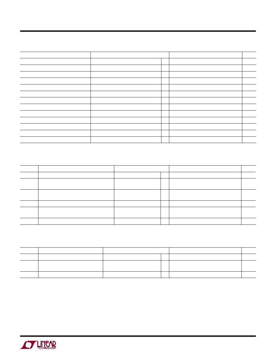
CONVERTER AND MULTIPLEXER CHARACTERISTICS
SYMBOL
PARAMETER
CONDITIONS
MIN
TYP
MAX
UNITS
VIN+
Absolute Input Range (CH0, CH1, IN+)
(Note 9)
l
–0.05
REFCOMP
V
VIN–
Absolute Input Range (CH0, CH1, IN–)
Unipolar (Note 9)
Bipolar (Note 9)
l
–0.05
0.25 REFCOMP
0.75 REFCOMP
V
VIN+ – VIN– Input Differential Voltage Range
VIN = VIN+ – VIN– (Unipolar)
VIN = VIN+ – VIN– (Bipolar)
l
0 to VREF
±VREF/2
V
IIN
Analog Input Leakage Current
l
±1
μA
CIN
Analog Input Capacitance
Sample Mode
Hold Mode
55
5
pF
CMRR
Input Common Mode Rejection Ratio
70
dB
The
l denotes the specications
which apply over the full operating temperature range, otherwise specications are at TA = 25°C. (Notes 4, 5)
PARAMETER
CONDITIONS
MIN
TYP
MAX
UNITS
Resolution (No Missing Codes)
l
12
Bits
Integral Linearity Error
(Note 6)
l
±0.3
±1
LSB
Differential Linearity Error
l
±0.25
±1
LSB
Bipolar Zero Error
(Note 7)
l
±1
±6
LSB
Bipolar Zero Error Drift
0.002
LSB/°C
Unipolar Zero Error
(Note 7)
l
±1
±6
LSB
Unipolar Zero Error Drift
0.002
LSB/°C
Unipolar Zero Error Match (LTC2306)
±0.3
±3
LSB
Bipolar Full-Scale Error
(Note 8)
l
±1.5
±8
LSB
Bipolar Full-Scale Error Drift
0.05
LSB/°C
Unipolar Full-Scale Error
(Note 8)
l
±1.2
±6
LSB
Unipolar Full-Scale Error Drift
0.05
LSB/°C
Unipolar Full-Scale Error Match (LTC2306)
±0.3
±3
LSB
ANALOG INPUT The l denotes the specications which apply over the full operating temperature range, otherwise
specications are at TA = 25°C. (Note 4)
SYMBOL
PARAMETER
CONDITIONS
MIN
TYP
MAX
UNITS
VREF Input Range
l
0.1
VDD
V
IREF
Reference Input Current
fSMPL = 0ksps, VREF = 4.096V
fSMPL = 500ksps, VREF = 4.096V
l
50
230
80
260
μA
CREF
Reference Input Capacitance
55
pF
REFERENCE INPUT The l denotes the specications which apply over the full operating temperature range,
otherwise specications are at TA = 25°C. (Note 4)
发布紧急采购,3分钟左右您将得到回复。
相关PDF资料
LTC2351HUH-12#TRPBF
IC ADC 12BIT 1.5MSPS 32-QFN
LTC2351HUH-14#TRPBF
IC ADC 14BIT 1.5MSPS 32-QFN
LTC2355IMSE-14#TRPBF
IC ADC 14BIT 3.5MSPS 10-MSOP
LTC2356IMSE-14#TRPBF
IC ADC 14BIT 3.5MSPS 10-MSOP
LTC2366HTS8#TRPBF
IC ADC 12BIT 3MSPS TSOT23-8
LTC2379HMS-18#PBF
IC ADC 18BIT SPI/SRL 16MSOP
LTC2380HMS-16#TRPBF
IC ADC 16BIT 2MSPS 16-MSOP
LTC2382HMS-16#PBF
IC ADC 16BIT 1CH 500KSPS 16-MSOP
相关代理商/技术参数
LTC2306CDD#TRPBF
功能描述:IC ADC 12-BIT 2CH 500KSPS 10DFN RoHS:是 类别:集成电路 (IC) >> 数据采集 - 模数转换器 系列:- 标准包装:2,500 系列:- 位数:16 采样率(每秒):15 数据接口:MICROWIRE?,串行,SPI? 转换器数目:1 功率耗散(最大):480µW 电压电源:单电源 工作温度:-40°C ~ 85°C 安装类型:表面贴装 封装/外壳:38-WFQFN 裸露焊盘 供应商设备封装:38-QFN(5x7) 包装:带卷 (TR) 输入数目和类型:16 个单端,双极;8 个差分,双极 配用:DC1011A-C-ND - BOARD DELTA SIGMA ADC LTC2494
LTC2306IDD#PBF
功能描述:IC ADC 12BIT 2CH 500KSPS 10-DFN RoHS:是 类别:集成电路 (IC) >> 数据采集 - 模数转换器 系列:- 标准包装:2,500 系列:- 位数:16 采样率(每秒):15 数据接口:MICROWIRE?,串行,SPI? 转换器数目:1 功率耗散(最大):480µW 电压电源:单电源 工作温度:-40°C ~ 85°C 安装类型:表面贴装 封装/外壳:38-WFQFN 裸露焊盘 供应商设备封装:38-QFN(5x7) 包装:带卷 (TR) 输入数目和类型:16 个单端,双极;8 个差分,双极 配用:DC1011A-C-ND - BOARD DELTA SIGMA ADC LTC2494
LTC2306IDD#TRPBF
功能描述:IC ADC 12-BIT 2CH 500KSPS 10DFN RoHS:是 类别:集成电路 (IC) >> 数据采集 - 模数转换器 系列:- 标准包装:2,500 系列:- 位数:16 采样率(每秒):15 数据接口:MICROWIRE?,串行,SPI? 转换器数目:1 功率耗散(最大):480µW 电压电源:单电源 工作温度:-40°C ~ 85°C 安装类型:表面贴装 封装/外壳:38-WFQFN 裸露焊盘 供应商设备封装:38-QFN(5x7) 包装:带卷 (TR) 输入数目和类型:16 个单端,双极;8 个差分,双极 配用:DC1011A-C-ND - BOARD DELTA SIGMA ADC LTC2494
LTC2308CUF#PBF
功能描述:IC ADC 12BIT 8CH 500KSPS 24-QFN RoHS:是 类别:集成电路 (IC) >> 数据采集 - 模数转换器 系列:- 标准包装:1,000 系列:- 位数:16 采样率(每秒):45k 数据接口:串行 转换器数目:2 功率耗散(最大):315mW 电压电源:模拟和数字 工作温度:0°C ~ 70°C 安装类型:表面贴装 封装/外壳:28-SOIC(0.295",7.50mm 宽) 供应商设备封装:28-SOIC W 包装:带卷 (TR) 输入数目和类型:2 个单端,单极
LTC2308CUF#PBF
制造商:Linear Technology 功能描述:A/D Converter (A-D) IC
LTC2308CUF#TRPBF
功能描述:IC ADC 12BIT 500KSPS 24-QFN RoHS:是 类别:集成电路 (IC) >> 数据采集 - 模数转换器 系列:- 标准包装:1,000 系列:- 位数:16 采样率(每秒):45k 数据接口:串行 转换器数目:2 功率耗散(最大):315mW 电压电源:模拟和数字 工作温度:0°C ~ 70°C 安装类型:表面贴装 封装/外壳:28-SOIC(0.295",7.50mm 宽) 供应商设备封装:28-SOIC W 包装:带卷 (TR) 输入数目和类型:2 个单端,单极
LTC2308CUFPBF
制造商:Linear Technology 功能描述:ADC 12-Bit 8-Ch 500Ksps Low Noise QFN24
LTC2308IUF#PBF
功能描述:IC ADC 12BIT 8CH 500KSPS 24-QFN RoHS:是 类别:集成电路 (IC) >> 数据采集 - 模数转换器 系列:- 标准包装:1 系列:microPOWER™ 位数:8 采样率(每秒):1M 数据接口:串行,SPI? 转换器数目:1 功率耗散(最大):- 电压电源:模拟和数字 工作温度:-40°C ~ 125°C 安装类型:表面贴装 封装/外壳:24-VFQFN 裸露焊盘 供应商设备封装:24-VQFN 裸露焊盘(4x4) 包装:Digi-Reel® 输入数目和类型:8 个单端,单极 产品目录页面:892 (CN2011-ZH PDF) 其它名称:296-25851-6